
Products
The development of the CMOS inverter marked a significant turning point in technology history, providing essential functionality for integrated circuits. This logic circuit showcases the unique electrical properties of CMOS, making it particularly suitable for high-density, high-performance digital systems. One of the primary advantages of CMOS technology is its efficiency: current flows only during state transitions, meaning that when a CMOS circuit maintains a logic high or low, it consumes very little power. This low power dissipation is especially beneficial when trying to integrate as much transistor functionality as possible into a compact space.
Effective heat dissipation is critical for integrated circuits, and the CMOS inverter plays a vital role in this process. In this first part of a three-part series, we will review the key characteristics of the CMOS inverter and discuss its two main types of power dissipation: dynamic power and static power. Subsequent articles will delve deeper into the mechanisms of dynamic power dissipation.
A CMOS inverter consists of an NMOS transistor and a PMOS transistor connected in a complementary manner. The schematic diagram in Figure 1 illustrates the structure of a basic CMOS inverter.
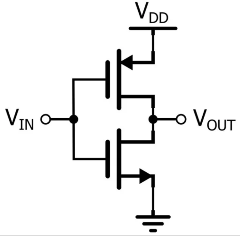
A CMOS inverter consists of an NMOS transistor and a PMOS transistor connected in a specific configuration. The operation is straightforward: when a logic high voltage is applied to the input terminal, the PMOS transistor turns off, and the NMOS transistor turns on, resulting in the output connecting to ground (0 V) through a low-resistance path. Conversely, when the input is at a logic low voltage, the PMOS conducts while the NMOS turns off, connecting the output to VDD, thus producing a logic high output. This inversion characteristic enables the CMOS inverter to effectively implement logical operations.
Power is consumed whenever current flows, as represented by the fundamental power formula P=I×VP = I \times VP=I×V. Although a CMOS inverter does not consume significant power in its steady state, it does incur dynamic power loss during logic transitions, primarily categorized into switching power and short-circuit power dissipation.
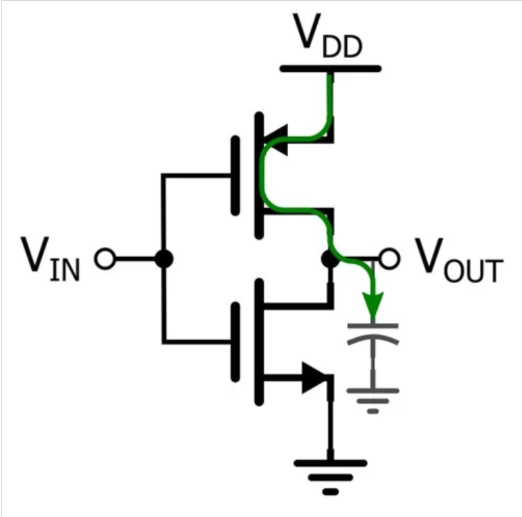
When a logic transition occurs at the input, transient current flows to charge or discharge the circuit's capacitance. During a transition from low to high output, current charges the load capacitance as the output voltage rises to VDD. Figure 2 illustrates the current path during this process.
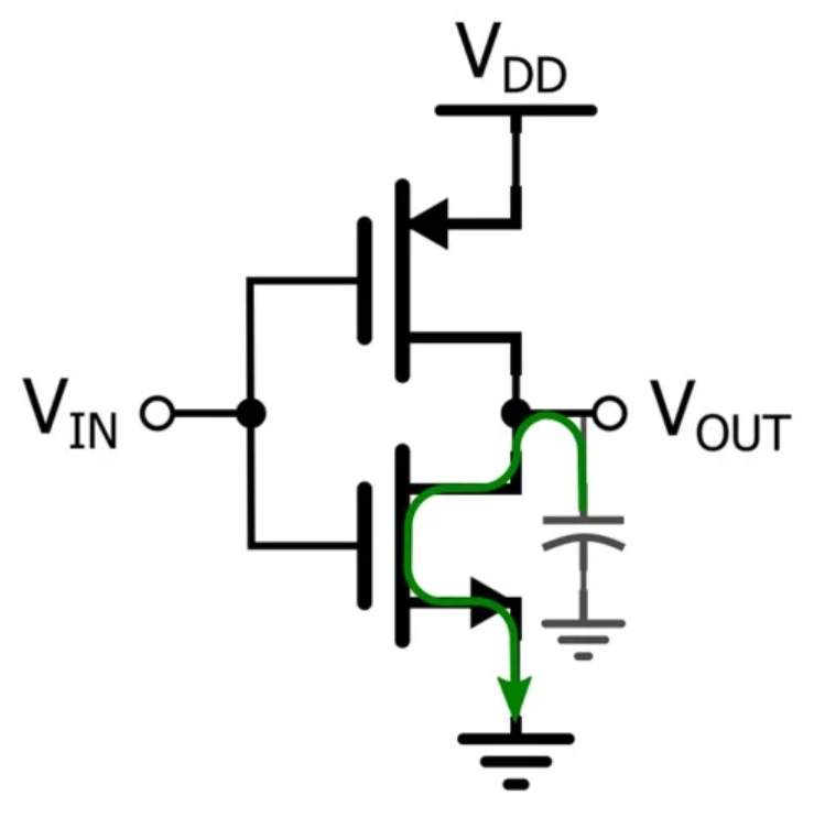
Current also flows during a high-to-low output transition (see Figure 3), discharging the capacitance as the output voltage drops to ground potential.
When a logic input changes, transient current flows to charge or discharge the circuit's capacitance. During a transition from low to high output, current flows to charge the load capacitance until the output voltage rises to VDD. The switching power dissipation can be estimated using the formula Pswitching=CL×VDD2×fP_{switching} = C_{L} \times V_{DD}^{2} \times fPswitching=CL×VDD2×f, where CLC_{L}CL represents the load capacitance and fff is the switching frequency. This formula indicates that increases in either switching frequency or load capacitance will lead to higher power consumption.
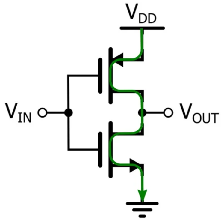
Short-circuit power dissipation occurs during the inverter's state transitions when both NMOS and PMOS transistors briefly conduct. This momentary overlap creates a direct path for current to flow from VDD to ground, resulting in energy loss. Although this condition lasts only briefly, it can significantly impact overall power consumption, especially in high-speed applications (Figure 4).
Even in a steady state, a CMOS inverter is not entirely free from power consumption. Field-effect transistors are not ideal switches; therefore, leakage currents can still flow from the source to the drain or substrate, even when off. Static power dissipation can be calculated using the formula Pstatic=Ileakage×VDDP_{static} = I_{leakage} \times V_{DD}Pstatic=Ileakage×VDD, where IleakageI_{leakage}Ileakage is the magnitude of the leakage current. As technology advances and the sizes of CMOS features decrease, static power consumption has become more significant, often approaching dynamic power levels. Moreover, static power is temperature-dependent; as operating temperature increases, leakage currents rise, further increasing static power dissipation.
The CMOS inverter is crucial for both standalone logic operations and as a fundamental component in more complex digital circuits. It provides buffering at the outputs, enhancing signal integrity and reducing rise and fall times, while also restoring signals to full logic levels. In this article, we briefly discussed the operation of the CMOS inverter and examined its dynamic and static power dissipation characteristics. In the upcoming articles, we will use LTspice simulations to explore dynamic power dissipation in greater detail.
Previous: TinyML in Action: Building a Voice-Controlled Robotic Subsystem
Next: Electromagnetic Side-Channel Attacks on Cryptographic Systems