
Products
There was a time when discrete components such as resistors, capacitors, inductors, transistors, and diodes sufficed for many electrical design projects. Today, however, it's uncommon to find a circuit board without at least one integrated circuit (IC), and many boards are packed with ICs of various shapes and sizes. The widespread use of ICs in contemporary electrical engineering is closely tied to the vast selection of microchips that engineers can easily locate, evaluate, purchase, and implement. Nevertheless, off-the-shelf ICs sometimes fail to deliver an optimized solution, prompting engineers to explore the option of using application-specific integrated circuits (ASICs).
There is no official consensus on the precise definition of an ASIC, and even among electronics professionals, there may be differing opinions about what constitutes an ASIC or whether a specific component qualifies as one. However, I believe the following definition from an old issue of Analog Dialogue (p. 12) serves as an excellent starting point: an ASIC is defined as an integrated circuit designed for a specific customer, application, or market using cell-based techniques, where necessary functional blocks are drawn from a cell library, interconnected, and simulated to deliver the desired system functions and performance level. This definition notably excludes ICs designed using conventional “custom” design techniques.
The initial part of this definition—an IC designed for a specific customer, application, or market—provides a broader and perhaps more commonly accepted understanding of the term. The latter part of the definition is particularly useful as it differentiates “ASIC” from the more general category of “custom IC.” If ASIC and custom IC are synonymous, then what is the need for the term ASIC?
The complete definition clarifies that an ASIC is an IC offering customized functionality without necessitating a fully bespoke design process. Instead, this customization is achieved through a process similar to PCB design. When creating a schematic, components are selected from a library and interconnected, and portions of the schematic may be verified through simulation. In the case of an ASIC, designers take functional blocks from a library, interconnect them, and verify both functionality and performance through simulation.
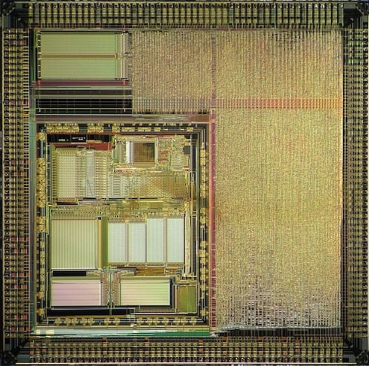
For instance, Figure 1 illustrates an ASIC that integrates a standard digital signal processor (DSP) core with additional circuitry tailored for a specific application.
The term “application specific” in ASIC can be somewhat misleading. In contemporary electrical engineering terminology, “application” typically refers to the practical use of electrical equipment. In essence, the application of an electrical device addresses the question: what useful work is this device designed to perform?
For example, in his introductory article on filters, Nick Davis outlines that filter applications encompass radio communications, DC power supplies, and audio electronics. This indicates that filter circuits are valuable in systems aimed at enabling wireless communication, generating stable supply voltages, or producing high-quality sound.
Interestingly, application-specific integrated circuits often are not confined to a single application or may not be limited to a specific use. A highly integrated data converter ASIC, for example, might be primarily designed for medical imaging applications, yet it could also serve effectively in industrial video processing or a multichannel automotive sensor network. Even more broadly, consider a system-on-chip (SoC) ASIC initially developed for smartphones; it may incorporate enough functionality to thrive across diverse applications.
Thus, alternative terms like task-specific integrated circuit (TSIC) or functionality-specific integrated circuit (FSIC) might offer more accuracy. However, TSIC and FSIC certainly lack the same appeal as ASIC. Generally, an ASIC is crafted to enable a single chip to efficiently carry out a particular combination of tasks. Even if this task combination is primarily necessary for one application, there may be various other contexts where the ASIC proves to be an effective and attractive alternative to off-the-shelf ICs.
Designing and verifying a customized IC, even with the assistance of functional blocks from a cell library, is no trivial task. If a designer cannot find the necessary functionality or performance in off-the-shelf ICs, the first instinct is usually to “keep looking.” If difficulties continue, employing programmable logic—such as a field-programmable gate array (FPGA) or complex programmable logic device (CPLD)—may present a feasible solution.
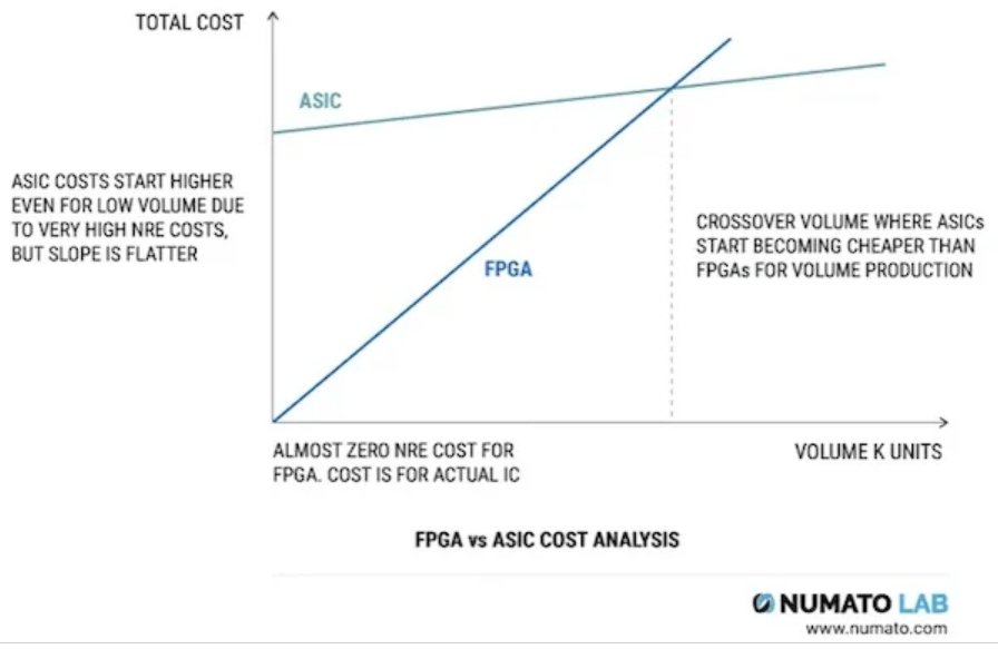
Developing an ASIC can entail months or even years of effort and millions of dollars in non-recurring engineering (NRE) costs before a single chip is produced. Consequently, high-volume projects with stringent performance requirements are typically scenarios where management can justify the investment of time and resources in ASIC development. With sufficient production volume, ASICs can become economically advantageous. Overall production costs decrease because the reduction in component and assembly expenses outweighs the addition of the amortized ASIC development costs. This can be illustrated in Figure 3.
Here’s a brief outline of the major stages involved in an ASIC design project:
· Define the ASIC specifications based on system requirements and constraints.
· Use the specifications to establish a high-level architectural design.
· Implement the high-level architecture as low-level logic. As with FPGAs and CPLDs, hardware description languages (like VHDL and Verilog) have become essential tools for ASIC design.
· Test the design to confirm functionality and timing.
· Translate the logical design into a physical layout.
· Once the physical layout is validated, the project is prepared for tape-out and fabrication.
· Following successful fabrication and packaging, the ASIC undergoes electrical testing and integration into prototypes for both lab and field testing.
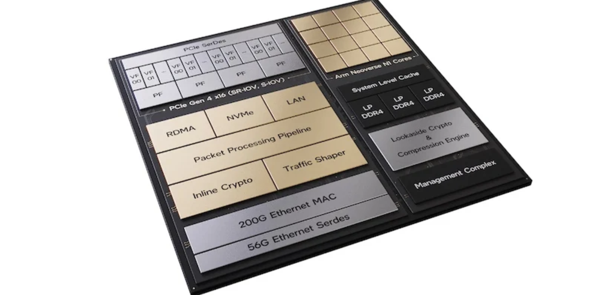
Figure 3 provides an example of an ASIC diagram. It illustrates the high-level architecture of an ASIC developed by Intel and Google, which functions as a “programmable networking device” for “cloud and communication service providers.” For further details, refer to the corresponding article. This is just one instance of a device that has undergone the ASIC design process.
In summary, ASICs are crucial components in the realm of high-performance and high-volume electronic devices that cannot be optimally designed using off-the-shelf components.
Have you ever participated in ASIC development? Or do you have experiences analyzing whether an ASIC would be economically feasible for a specific project? Feel free to share your thoughts in the comments!
Previous: How to Determine the Number of Hidden Layers and Nodes in a Neural Network?
Next: TinyML in Action: Building a Voice-Controlled Robotic Subsystem